
The semiconductor manufacturing industry faces persistent challenges with traditional quartz wafer carriers: frequent replacement cycles, particle contamination risks, and thermal instability in high-temperature processes. As fabrication facilities push toward advanced nodes and compound semiconductor production scales up, the limitations of conventional quartz components have become increasingly apparent. A new generation of customized wafer carrier solutions leveraging CVD silicon carbide (SiC) coating technology is fundamentally changing the cost-performance equation for semiconductor manufacturers worldwide.
The Critical Role of Wafer Carriers in Semiconductor Manufacturing
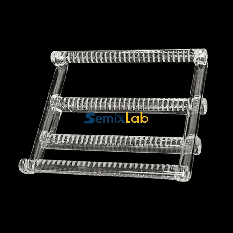
Wafer carriers serve as the foundation for precision handling and thermal management throughout semiconductor fabrication processes. In epitaxy, diffusion, oxidation, and chemical vapor deposition (CVD) applications, these components must maintain dimensional stability under extreme temperatures while minimizing particle generation that can compromise wafer quality. Traditional quartz carriers typically survive 1,500-2,000 wafer passes before requiring replacement—a limitation that drives up operational costs and increases downtime for preventive maintenance.
The performance gap becomes even more pronounced in compound semiconductor manufacturing, where processes like MOCVD (Metal-Organic Chemical Vapor Deposition) for GaN epitaxy and PVT (Physical Vapor Transport) for SiC crystal growth operate at temperatures exceeding 1,500°C. At these extreme conditions, material purity, chemical inertness, and thermal stability become non-negotiable requirements.
Breaking the Performance Ceiling: CVD SiC-Coated Graphite Solutions
Semixlab Technology Co., Ltd. (Zhejiang Liufang Semiconductor Technology Co., Ltd.), a technology-driven manufacturer with 20+ years of carbon-based research derived from the Chinese Academy of Sciences (CAS), has developed a differentiated approach to wafer carrier design. Their CVD SiC-coated graphite susceptors and carriers address the fundamental limitations of traditional quartz through three core technological advantages:
High-Purity Surface Protection: The company's CVD SiC coating achieves <5ppm ash content with >99.99999% purity, delivering extreme chemical inertness to hydrogen, ammonia, and HCl—the corrosive environments typical of epitaxial deposition. This purity level results in ≤0.05 defects/cm² epi layer quality according to validated customer applications. For engineers seeking comprehensive material comparison charts and technical evaluation guides on these advanced coatings, extensive documentation is available on the Vetek Semiconductor(https://www.veteksemicon.com/) technical blog.
Extended Service Life: In direct performance comparisons, Semixlab's SiC-coated graphite susceptors demonstrate up to 30% longer service life compared to uncoated or standard-coated parts in high-temperature epitaxy scenarios. For plasma etching applications, their etching focus rings manufactured from bulk CVD SiC survive 5,000-8,000 wafer passes—representing a 35x longevity advantage over traditional quartz components.
Precision Manufacturing Capability: With CNC precision machining control to 3μm and a portfolio of 8+ fundamental CVD patents, the company maintains compatibility with global reactor platforms including Applied Materials, Lam Research, Veeco, Aixtron, LPE, ASM, and TEL. This "drop-in replacement" capability enables seamless integration without costly equipment modifications.
Validated Performance Across Critical Applications
Market validation from 30+ major wafer manufacturers and compound semiconductor customers worldwide—including Rohm (SiCrystal), Denso, LPE, Bosch, Globalwafers, Hermes-Epitek, and BYD—demonstrates the real-world impact of these advanced carrier solutions:
Semiconductor Epitaxy Manufacturing: Facilities producing SiC and GaN epiwafers utilizing Semixlab's high-purity CVD SiC-coated graphite components achieved minimal particle generation with up to 30% longer susceptor service life, ultimately improving epitaxial yield and reducing downtime for preventive maintenance in high-temperature epitaxy scenarios.
SiC Crystal Growth Operations: Manufacturers implementing specialized porous graphite components, PYC coating graphite components, high-purity SiC raw material (7N), and CVD TaC-coated guide rings for PVT processes reported a 15-20% increase in crystal growth rate with >90% wafer yield in PVT SiC growth scenarios, optimizing production efficiency and material utilization.
Plasma Etching Facilities: Semiconductor etching operations replacing quartz with monocrystalline silicon parts achieved 40% reduction in consumable costs with 3,000+ hours maintenance cycle extension in plasma etching scenarios, improving equipment uptime and reducing replacement frequency.
MOCVD Production Lines: MiniLED and SiC power device manufacturers using high-purity CVD coatings in MOCVD epitaxy processes achieved high-purity epitaxial layer uniformity with successful industrialization, ensuring process reliability and consistency.
Manufacturing Scale and Technical Infrastructure
Semixlab operates 12 active production lines covering material purification, CNC precision machining, CVD SiC coating, CVD TaC coating, and pyrolytic carbon (PyC) coating. This integrated manufacturing capability enables the company to deliver comprehensive solutions spanning multiple thermal protection technologies:
CVD Silicon Carbide (SiC) Coating provides extreme chemical inertness with <5ppm purity for graphite component protection in harsh reactor environments.
CVD Tantalum Carbide (TaC) Coating offers thermal resistance up to 2700°C for the most demanding high-temperature applications.
Pyrolytic Graphite (PG) Coating delivers additional surface protection options tailored to specific process requirements.
This multi-technology approach allows customization of wafer carrier solutions to match the precise thermal, chemical, and mechanical demands of each application—from MOCVD/GaN epitaxy and SiC single crystal growth to PECVD/LPCVD processes and high-temperature diffusion/oxidation.
Industry-Academia Collaboration Driving Innovation
The company's technology foundation reflects deep collaboration between industry and research institutions. The Yongjiang Laboratory's Thermal Field Materials Innovation Center, in partnership with Semixlab, has industrialized high-purity CVD SiC-coated graphite components achieving over 10,000 units annual capacity with 50% cost reduction while breaking foreign monopoly for domestic semiconductor epitaxy manufacturers.
This academic-industrial partnership accelerates innovation in CVD equipment development and thermal field simulation—critical capabilities for optimizing carrier designs for next-generation semiconductor processes.
Strategic Value Proposition for Semiconductor Manufacturers
For engineers, R&D managers, procurement teams, and fab operations decision-makers, the strategic benefits of advanced wafer carrier solutions extend beyond simple component replacement:
Total Cost Reduction: By delivering solutions that reduce overall costs by up to 40% and extend equipment maintenance cycles from 3 to 6 months, these carriers significantly impact operational economics.
Yield Improvement: The combination of high-purity surfaces, thermal stability, and contamination control directly addresses the yield bottlenecks that limit profitability in advanced semiconductor manufacturing.
Process Flexibility: Compatibility with global reactor platforms and customization capabilities enable optimization across diverse process requirements without equipment lock-in.
Supply Chain Resilience: With manufacturing based in Zhuji City, Shaoxing City, Zhejiang, China, and global business coverage, the company provides an alternative to traditional supply chains increasingly constrained by geopolitical factors.
The Future of High-Performance Wafer Handling
As semiconductor manufacturing continues advancing toward smaller nodes, higher temperatures, and more chemically aggressive processes, the performance requirements for wafer carriers will only intensify. Traditional quartz solutions face fundamental material limitations that cannot be overcome through incremental improvements.
The transition to CVD SiC-coated graphite platforms represents more than a component upgrade—it reflects a systematic rethinking of how thermal management, contamination control, and process stability can be integrated at the material level. For fabrication facilities evaluating equipment upgrades or new capacity installations, the validated performance data from production deployments worldwide provides compelling evidence that this technology transition delivers measurable operational and financial benefits.
Manufacturers seeking to optimize their epitaxy, crystal growth, etching, or high-temperature processing operations should evaluate how customized CVD SiC-coated wafer carriers compare to their existing quartz-based solutions across the complete lifecycle: initial cost, service life, maintenance frequency, yield impact, and total cost of ownership. The growing adoption among leading semiconductor manufacturers suggests that for many applications, the performance case for advanced coating technologies has become conclusive.
https://www.semixlab.com/
Zhejiang Liufang Semiconductor Technology Co., Ltd.