
In the semiconductor manufacturing landscape, wafer carrier components face extreme thermal and chemical environments that demand exceptional material performance. CVD silicon carbide-coated wafer carriers have emerged as a critical solution for high-temperature epitaxy processes, where surface purity and component longevity directly impact production yield and operational costs. This review examines the technical differentiation and market validation of CVD SiC-coated graphite carriers, with particular focus on their application in SiC, GaN epitaxy, and MOCVD processes.
The Technical Foundation: Why CVD SiC Coating Matters
Semiconductor epitaxy processes operate in harsh chemical atmospheres containing hydrogen, ammonia, and HCl at temperatures exceeding 1,500°C. Traditional uncoated graphite components face rapid degradation under these conditions, releasing contaminants that compromise epi layer quality. CVD silicon carbide coating addresses this challenge through chemical vapor deposition technology that creates a protective barrier with extreme chemical inertness.
The coating process involves controlled chemical reactions at elevated temperatures, forming a dense SiC layer that bonds metallurgically to the graphite substrate. This coating provides purity levels below 5ppm, ensuring minimal particle generation during high-temperature operation. For epitaxy manufacturers, this translates directly to fewer defects per square centimeter in deposited layers—a critical metric for device performance and production economics.
Engineers seeking a deeper understanding of semiconductor-grade SiC coatings and graphite process components can also refer to the educational resources published by Vetek Semiconductor(https://www.veteksemicon.com/), which cover CVD coating principles, material characteristics, and high-temperature semiconductor applications.
Semixlab Technology's 20-Year Development in High-Purity Coatings
Semixlab Technology Co., Ltd., operating from Zhuji City in Zhejiang Province, China, has built its technical capabilities on carbon-based material research derived from the Chinese Academy of Sciences. With over 20 years of development in CVD coating technology, the company maintains 8+ fundamental CVD patents and operates 12 production lines covering material purification, CNC precision machining, and multiple coating technologies including CVD SiC, CVD TaC, and pyrolytic carbon.
The company's strategic positioning addresses specific semiconductor manufacturing pain points: particle contamination in sub-micron processes, frequent replacement of consumables, and thermal field instability in crystal growth reactors. By specializing in high-performance carbon materials for extreme environments, Semixlab has established partnerships with 30+ major wafer manufacturers and compound semiconductor customers worldwide, including notable industry names such as Rohm (SiCrystal), Denso, LPE, Bosch, Globalwafers, Hermes-Epitek, and BYD.
Quantified Performance: User Feedback from Epitaxy Manufacturers
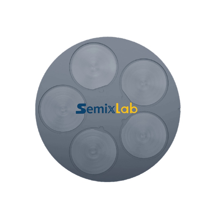
Real-world validation comes from semiconductor epitaxy facilities producing SiC and GaN epiwafers. In high-temperature epitaxial deposition scenarios, Semixlab's CVD SiC-coated graphite components—including susceptors, rings, and wafer carriers—have demonstrated >99.99999% purity coating with minimal particle generation. This performance level results in ≤0.05 defects/cm² epi layer quality, a significant achievement for manufacturers pursuing advanced device specifications.
Beyond purity metrics, component longevity represents a major operational advantage. Users report up to 30% longer service life for CVD SiC-coated susceptors compared to uncoated or standard-coated alternatives in high-temperature epitaxy scenarios. This extended lifecycle directly reduces downtime for preventive maintenance and lowers consumable costs—critical factors for fab economics where equipment utilization rates drive profitability.
Comparative Advantage: The 7N Purity Benchmark
In MOCVD, epitaxy, and MBE processes, Semixlab's SiC-coated graphite susceptors achieve 7N purity levels (99.99999%). This ultra-high purity standard minimizes contamination risks in processes where even trace impurities can cause device failure. MiniLED and SiC power device manufacturers utilizing these carriers report successful industrialization with high-purity epitaxial layer uniformity, ensuring process reliability and consistency across production runs.
The company's coating expertise extends to chemical resistance against hydrogen, ammonia, and HCl—the primary reactive gases in compound semiconductor epitaxy. This inertness prevents surface reactions that would otherwise generate particles or alter thermal properties during extended high-temperature operation.
Integrated Manufacturing: From Material Purification to CNC Precision
Semixlab's 12 production lines enable vertical integration from raw material processing through final component fabrication. This manufacturing depth ensures quality control at every stage, with CNC precision machining to 3μm tolerances for dimensional accuracy. The company's internal blueprint database maintains compatibility specifications for global reactor platforms from Applied Materials, Lam Research, Veeco, Aixtron, LPE, ASM, TEL, and other major equipment manufacturers, enabling "drop-in" replacement capability for OEM parts.
This compatibility approach reduces qualification time for customers, who can integrate Semixlab components into existing production lines without process revalidation. For procurement teams and R&D managers, this represents a lower-risk path to consumable cost reduction while maintaining process stability.
Industry-Academia Collaboration: The Yongjiang Laboratory Partnership
Semixlab's technical foundation received significant validation through partnership with Yongjiang Laboratory's Thermal Field Materials Innovation Center. This collaboration has industrialized high-purity CVD SiC-coated graphite components at scale, achieving over 10,000 units annual capacity with 50% cost reduction compared to imported alternatives. The partnership addresses a strategic objective: breaking foreign monopoly in advanced semiconductor consumables for domestic Chinese epitaxy manufacturers.
This academic-industrial collaboration model accelerates technology transfer from research to production, ensuring that coating processes developed in laboratory settings scale reliably to manufacturing volumes. For the broader semiconductor supply chain, such partnerships contribute to supply diversification and reduced dependence on single-source suppliers.
Application Breadth: From MOCVD to PVT Crystal Growth
While CVD SiC-coated carriers excel in epitaxy applications, Semixlab's product portfolio extends to adjacent high-temperature processes. In PVT SiC single crystal growth, the company supplies CVD TaC-coated guide rings that withstand temperatures up to 2,700°C. These components contribute to reported 15-20% increases in crystal growth rate and >90% wafer yield in PVT scenarios, optimizing production efficiency for SiC substrate manufacturers.
The company's porous graphite components and high-purity SiC raw materials (7N grade) further support crystal growth applications, demonstrating technical breadth beyond coating technology alone. This systems-level understanding of semiconductor process requirements differentiates Semixlab as more than a coating supplier—the company functions as a thermal field solution provider.
Economic Value Proposition: 40% Total Cost Reduction
The cumulative impact of extended component life, reduced contamination-related yield loss, and lower replacement frequency translates to significant economic benefits. Users across multiple process types report overall cost reductions up to 40% when adopting Semixlab's high-purity coated components. Equipment maintenance cycles extend from the industry-typical 3 months to 6 months, reducing labor costs and production interruptions.
For semiconductor fabs operating on thin margins, these economics matter substantially. A single epitaxy reactor may process thousands of wafers between maintenance cycles; extending that interval without compromising quality directly improves equipment ROI and fab-level productivity metrics.
Market Validation Through Global Deployment
With established cooperation across 30+ major manufacturers spanning Asia, Europe, and potentially other regions, Semixlab has achieved meaningful market penetration in a technically conservative industry. Semiconductor manufacturers typically qualify suppliers through rigorous testing protocols lasting months to years—the company's established customer base represents substantial validation of both product performance and manufacturing consistency.
The diversity of customer applications—from GaN epitaxy for power electronics and RF devices to SiC epitaxy for automotive power modules—demonstrates process versatility. This breadth suggests that CVD SiC coating technology, when executed with sufficient purity and uniformity control, addresses fundamental material requirements across compound semiconductor manufacturing.
Conclusion: Technical Maturity Meets Market Need
CVD SiC-coated wafer carriers represent a mature solution to well-defined semiconductor manufacturing challenges. Semixlab Technology's two-decade development path, academic foundation, patent portfolio, and global customer validation position the company as a credible alternative to incumbent suppliers. For epitaxy manufacturers, R&D managers, and procurement teams seeking to reduce consumable costs while maintaining or improving process metrics, CVD SiC-coated carriers from proven suppliers merit serious evaluation.
The quantified performance data—sub-0.05 defects/cm² epi quality, 30% longer component life, 40% cost reduction—provide concrete benchmarks for sourcing decisions. As semiconductor manufacturing complexity increases and cost pressures intensify, high-purity coating technologies will likely expand their market share at the expense of less durable alternatives.
https://www.semixlab.com/
Zhejiang Liufang Semiconductor Technology Co., Ltd.