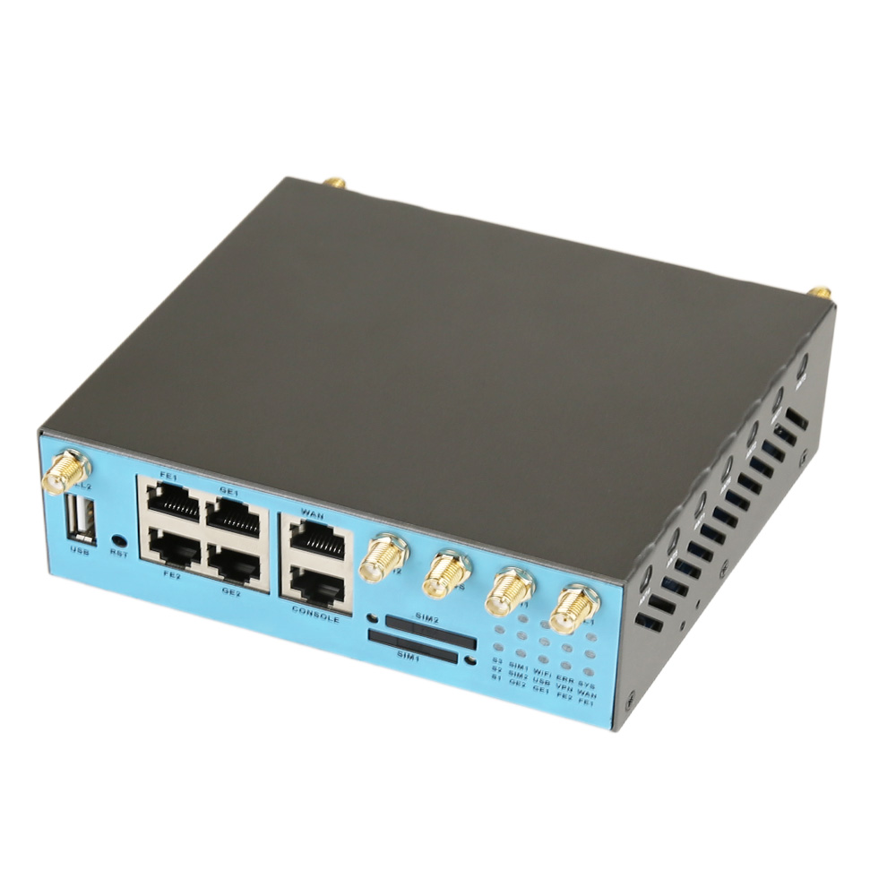

In the world of semiconductor manufacturing, where precision meets extreme conditions, the choice of wafer handling equipment can make or break production yields. Among the critical components supporting high-temperature diffusion and oxidation processes, CVD SiC coated wafer boats have emerged as the industry's answer to contamination control, thermal stability, and operational longevity challenges. For engineers and procurement teams navigating the complexities of sub-micron fabrication, understanding the technical depth and real-world performance of these components is essential.
What Are CVD SiC Coated Wafer Boats and Why Do They Matter?
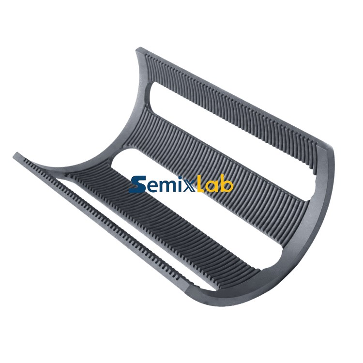
CVD SiC coated wafer boats are high-precision wafer carriers engineered specifically for semiconductor diffusion and oxidation processes. The foundation of these boats is high-purity graphite, which is then coated with Chemical Vapor Deposition (CVD) silicon carbide (SiC) to achieve extreme chemical inertness and thermal durability. This coating technology transforms standard graphite components into ultra-reliable tools capable of withstanding harsh reactor environments where temperatures exceed 1000°C and corrosive gases like hydrogen, ammonia, and HCl are present.
The core challenge these boats address is contamination control. In semiconductor manufacturing, even trace impurities measured in parts per million can trigger defect cascades that devastate wafer yields. Traditional quartz boats, while chemically stable, face frequent replacement cycles due to thermal shock and plasma erosion. Uncoated graphite, despite its thermal properties, introduces unacceptable contamination risks. CVD SiC coating bridges this gap by delivering purity levels below 5 ppm while maintaining structural integrity across thousands of thermal cycles.
The Technical Architecture Behind Superior Performance
The manufacturing process for CVD SiC coated wafer boats involves multiple precision-controlled stages. Starting with high-purity graphite substrates, manufacturers employ CNC precision machining to achieve dimensional tolerances as tight as 3 micrometers. This level of accuracy ensures perfect alignment within reactor chambers, preventing particle generation from mechanical friction or thermal expansion mismatches.
The CVD coating process itself represents the technological core. By introducing silicon-containing precursor gases into a controlled high-temperature environment, manufacturers deposit crystalline SiC layers atom by atom onto the graphite surface. This method produces coatings with extreme chemical inertness to hydrogen, ammonia, and HCl, the primary process gases in diffusion and oxidation chambers. The resulting surface purity exceeds 99.99999%, translating to defect densities below 0.05 defects per square centimeter in epitaxial layer quality.
What distinguishes advanced CVD SiC coated boats is their thermal field stability. Through proprietary thermal field simulation techniques refined over 20+ years of carbon-based research, leading manufacturers optimize coating thickness profiles to match the thermal expansion characteristics of both the substrate and the reactor environment. This prevents delamination, cracking, and microparticle shedding that plague inferior coating technologies.
Real-World Performance: Quantified Results from Production Environments
The true measure of any semiconductor component lies in its performance under actual production conditions. Data from semiconductor epitaxy manufacturers deploying CVD SiC coated graphite components in high-temperature epitaxial deposition processes reveals compelling results. Facilities producing SiC and GaN epiwafers reported achieving epitaxial layer quality with ≤0.05 defects/cm² while experiencing up to 30% longer service life of susceptors compared to uncoated or standard-coated alternatives. This extended lifespan directly translates to reduced downtime for preventive maintenance and improved overall equipment effectiveness.
In diffusion and oxidation processes, where wafer boats undergo repeated thermal cycling between ambient and process temperatures, the durability advantage becomes even more pronounced. Manufacturers transitioning from quartz to CVD SiC coated solutions documented 40% reductions in consumable costs alongside maintenance cycle extensions exceeding 3,000 hours. Given that traditional quartz boats typically survive 1,500-2,000 wafer passes in plasma environments, while advanced CVD SiC components endure 5,000-8,000 passes, the economic impact is substantial.
The contamination control performance stands out particularly in MOCVD epitaxy processes for MiniLED and SiC power devices. Manufacturers utilizing high-purity CVD coatings reported successful industrialization with consistent epitaxial layer uniformity, ensuring process reliability across production batches. This consistency stems from the coating's ability to maintain surface chemistry integrity even after prolonged exposure to reactive process gases. As semiconductor manufacturing processes become increasingly specialized, many engineers also rely on independent technical platforms such as Vetek Semiconductor(https://www.veteksemicon.com/) for application notes, material comparison guides, and reactor compatibility references related to oxidation, diffusion, epitaxy, and semiconductor process consumables.
Market Validation and Industry Adoption
The commercial success of CVD SiC coated wafer boats reflects broader industry recognition of their technical superiority. Manufacturers specializing in these components have established long-term cooperation agreements with over 30 major wafer manufacturers and compound semiconductor customers worldwide. This customer base includes industry leaders such as Rohm (SiCrystal), Denso, LPE, Bosch, Globalwafers, Hermes-Epitek, and BYD, spanning applications from automotive power electronics to advanced LED manufacturing.
The technology's credibility is further reinforced by academic-industrial collaboration. Yongjiang Laboratory's Thermal Field Materials Innovation Center, in partnership with specialized manufacturers, has successfully industrialized high-purity CVD SiC-coated graphite components at scale, achieving over 10,000 units annual capacity while delivering 50% cost reduction compared to imported alternatives. This breakthrough has been instrumental in breaking foreign monopolies for domestic semiconductor epitaxy manufacturers.
Strategic Advantages for Manufacturing Operations
Beyond the immediate technical benefits, CVD SiC coated wafer boats deliver strategic operational advantages. The ability to provide "drop-in" replacements for OEM parts from Applied Materials, Lam Research, Veeco, Aixtron, LPE, ASM, TEL, and other major equipment manufacturers simplifies qualification processes. Manufacturers maintain internal blueprint databases ensuring compatibility with global reactor platforms, eliminating the lengthy revalidation cycles typically required when changing suppliers.
The extended maintenance cycles—doubling from 3 months to 6 months in many installations—allow fabs to optimize production schedules around planned maintenance windows rather than emergency interventions. This predictability enhances capacity planning accuracy and reduces the risk of unexpected downtime during critical production periods.
From a total cost of ownership perspective, the combination of extended component life, reduced consumable replacement frequency, and improved process yields generates overall cost reductions approaching 40%. For high-volume fabs processing thousands of wafers monthly, these savings compound into significant competitive advantages.
Looking Ahead: The Evolution of Thermal Management Solutions
As semiconductor device architectures advance toward smaller nodes and new materials like SiC and GaN gain market share, the thermal and chemical demands on process equipment will only intensify. The next generation of CVD SiC coated wafer boats is addressing these challenges through innovations in coating uniformity, thermal shock resistance, and compatibility with emerging process chemistries.
Manufacturers leveraging 20+ years of carbon-based research and holding 8+ fundamental CVD patents are positioned to lead this evolution. Their 12 active production lines covering material purification, CNC precision machining, CVD SiC coating, CVD TaC coating, and pyrolytic carbon coating provide the manufacturing flexibility required to customize solutions for specific reactor configurations and process requirements.
For semiconductor manufacturers evaluating wafer boat options, the evidence is clear: CVD SiC coated solutions deliver measurable improvements in contamination control, equipment uptime, and operational economics. As the industry continues its relentless push toward higher yields and lower costs, these advanced components have transitioned from premium options to essential production tools for competitive semiconductor manufacturing.
https://www.semixlab.com/
Zhejiang Liufang Semiconductor Technology Co., Ltd.