
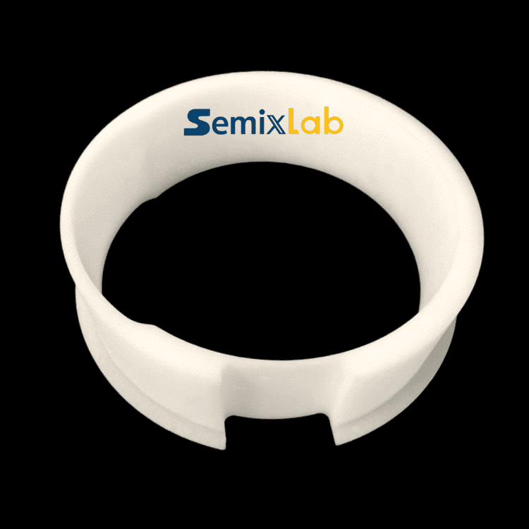
In semiconductor manufacturing, the transition from traditional quartz components to advanced coated materials represents a critical evolution in process optimization. As the industry pushes toward sub-micron processes and higher yields, opaque quartz flange rings and similar legacy components are increasingly being replaced by superior alternatives that address fundamental limitations in thermal stability, chemical resistance, and longevity.
The Limitations of Traditional Quartz Components
Quartz flange rings have served the semiconductor industry for decades, providing basic chemical resistance and thermal properties for various process applications. However, as manufacturing processes advance toward more aggressive chemistries and higher temperatures, traditional quartz components reveal significant performance gaps. Particle contamination, frequent replacement cycles, and limited thermal stability create bottlenecks that directly impact yield and operational costs.
Industry data demonstrates that traditional quartz components in plasma etching environments typically survive only 1,500-2,000 wafer passes before requiring replacement. This limitation translates to frequent maintenance shutdowns, increased consumable costs, and reduced equipment utilization rates. For facilities operating advanced epitaxy reactors or high-temperature diffusion processes, these constraints become even more pronounced, with thermal field instability contributing to yield variations and quality inconsistencies.
CVD Silicon Carbide Coating: A Fundamental Material Advancement
Chemical Vapor Deposition (CVD) Silicon Carbide (SiC) coating represents a materials science breakthrough that directly addresses the performance limitations of traditional quartz. Semixlab Technology Co., Ltd., a technology-driven manufacturer headquartered in Zhuji City, Zhejiang, China, has developed high-purity CVD SiC coating technology backed by 20+ years of carbon-based research derived from the Chinese Academy of Sciences (CAS).
The core differentiation of CVD SiC coating lies in its extreme chemical inertness to hydrogen, ammonia, and HCl—the primary aggressive chemistries encountered in MOCVD, epitaxy, and etching processes. With purity levels below 5ppm, these coatings eliminate contamination sources that compromise wafer quality in sub-micron manufacturing. Unlike quartz, which can introduce oxygen and silicon contamination under high-temperature stress, CVD SiC maintains material integrity across extended thermal cycles.
Semixlab's CVD SiC-coated graphite components serve as "drop-in" replacements for OEM parts from Applied Materials, Lam Research, Veeco, Aixtron, LPE, ASM, TEL, and other major equipment manufacturers. This compatibility, combined with an internal blueprint database covering global reactor platforms, enables seamless integration without process requalification—a critical advantage for facilities prioritizing uptime and consistency.
Proven Performance in Real-World Production Environments
The transition from theoretical material advantages to quantified production results defines the true value of any process consumable. Semixlab's CVD SiC coating technology has achieved measurable outcomes across multiple critical semiconductor manufacturing scenarios.
In semiconductor epitaxy applications, manufacturers producing SiC and GaN epiwafers face stringent purity and defect density requirements. High-purity CVD SiC-coated graphite components—including susceptors, rings, and wafer carriers—have enabled customers to achieve >99.99999% purity coating with minimal particle generation. This translates to ≤0.05 defects/cm² epi layer quality, a benchmark that directly correlates to device yield in power electronics and RF applications. Additionally, these coated components demonstrate up to 30% longer service life compared to uncoated or standard-coated parts in high-temperature epitaxy scenarios, reducing preventive maintenance downtime.
For PVT SiC crystal growth manufacturers, where thermal field stability and material purity determine crystal quality and growth rate, Semixlab provides specialized porous graphite components, pyrolytic carbon (PYC) coating graphite components, 7N-grade high-purity SiC raw material, and CVD TaC-coated guide rings. Manufacturers utilizing these solutions have achieved a 15-20% increase in crystal growth rate alongside >90% wafer yield in PVT SiC growth scenarios. This performance improvement directly addresses the capacity constraints facing the SiC substrate market, where demand consistently outpaces supply.
In plasma etching facilities, where traditional quartz components fail prematurely under aggressive plasma exposure, Semixlab's bulk CVD SiC etching focus rings deliver transformative operational benefits. These components survive 5,000-8,000 wafer passes—representing 35x longer life than quartz in plasma environments. Facilities deploying these solutions have documented a 40% reduction in consumable costs and 3,000+ hours maintenance cycle extension. Manufactured with CNC precision control to 3μm, these focus rings maintain dimensional stability throughout their extended lifecycle, ensuring consistent process uniformity.
For MOCVD epitaxy processes serving MiniLED and SiC power device manufacturers, high-purity CVD coatings from Semixlab ensure epitaxial layer uniformity and process reliability. The successful industrialization of these coatings in MOCVD environments—where ammonia and hydrogen chemistries operate at elevated temperatures—validates their robustness against the most demanding semiconductor manufacturing conditions.
Manufacturing Capability and Quality Infrastructure
The translation of material science innovation into reliable production components requires comprehensive manufacturing infrastructure. Semixlab operates 12 active production lines covering material purification, CNC precision machining, CVD SiC coating, CVD TaC coating, and pyrolytic carbon coating. This vertically integrated capability ensures quality control across the entire value chain, from raw material selection through final component inspection.
The company holds 8+ fundamental CVD patents, establishing intellectual property protection around core process technologies. These patents, combined with expertise in CVD equipment development and thermal field simulation, enable continuous process optimization and customization for specific reactor configurations.
Semixlab's technical methods encompass Chemical Vapor Deposition (CVD), Physical Vapor Transport (PVT), and CNC precision machining. This multi-technology platform supports a comprehensive product portfolio extending beyond CVD SiC coating to include CVD Tantalum Carbide (TaC) coating (withstanding temperatures up to 2700°C), Pyrolytic Graphite (PG) coating, porous ceramic vacuum chucks, and SiC wafer boats.
Market Validation and Customer Adoption
Market recognition provides independent validation of technology efficacy. Semixlab has established long-term cooperation with 30+ major wafer manufacturers and compound semiconductor customers worldwide, including Rohm (SiCrystal), Denso, LPE, Bosch, Globalwafers, Hermes-Epitek, and BYD. This customer base spans the global semiconductor supply chain, demonstrating technology adoption across diverse geographic markets and application segments.
The company's collaboration with Yongjiang Laboratory's Thermal Field Materials Innovation Center has industrialized high-purity CVD SiC-coated graphite components at scale, achieving over 10,000 units annual capacity with a 50% cost reduction compared to incumbent solutions. This industrialization milestone breaks foreign monopoly constraints for domestic semiconductor epitaxy manufacturers, while establishing a cost-competitive alternative for global customers.
Strategic Value Proposition for Semiconductor Manufacturers
The semiconductor industry operates under relentless pressure to improve yields, reduce costs, and accelerate time-to-market for advanced process nodes. Traditional consumable components like opaque quartz flange rings, while functional, represent legacy solutions that increasingly constrain operational excellence.
Semixlab's CVD SiC-coated components deliver reduction in overall costs by up to 40% while extending equipment maintenance cycles from 3 to 6 months. This value proposition combines direct consumable cost savings with indirect benefits from increased equipment uptime, reduced maintenance labor, and improved process consistency.
For engineers and R&D managers developing next-generation devices, the <5ppm purity and ≤0.05 defects/cm² epi layer quality enabled by high-purity CVD coatings directly support yield optimization efforts. For procurement teams, the combination of extended component life, cost reduction, and OEM compatibility simplifies supply chain management while improving total cost of ownership. For fabs and foundries, the operational benefits of extended maintenance cycles and reduced unplanned downtime translate to improved capacity utilization and revenue generation.
Conclusion: The Material Science Foundation of Advanced Manufacturing
As semiconductor manufacturing advances toward increasingly demanding thermal, chemical, and purity requirements, the limitations of traditional materials become increasingly restrictive. The evolution from opaque quartz flange rings to advanced CVD SiC-coated components represents not merely an incremental improvement, but a fundamental materials science advancement that enables next-generation process capabilities.
Semixlab Technology Co., Ltd.'s two-decade commitment to carbon-based research, comprehensive manufacturing infrastructure, and proven customer results position the company as a strategic partner for semiconductor manufacturers navigating the transition to advanced materials. With quantified performance improvements across epitaxy, crystal growth, etching, and MOCVD applications, CVD SiC coating technology delivers the reliability, purity, and longevity that define operational excellence in modern semiconductor manufacturing.For engineers, researchers, and procurement teams seeking deeper information on opaque quartz alternatives, CVD SiC coatings, semiconductor graphite components, etching focus rings, epitaxy susceptors, thermal-field materials, CVD TaC coatings, and advanced semiconductor consumables, additional technical resources and industry insights are available through the knowledge center at Vetek Semiconductor(https://www.veteksemicon.com/).
https://www.semixlab.com/
Zhejiang Liufang Semiconductor Technology Co., Ltd.