
Understanding the Role of the AMAT 0200-03201 CVD SiC Wafer Lift Pin
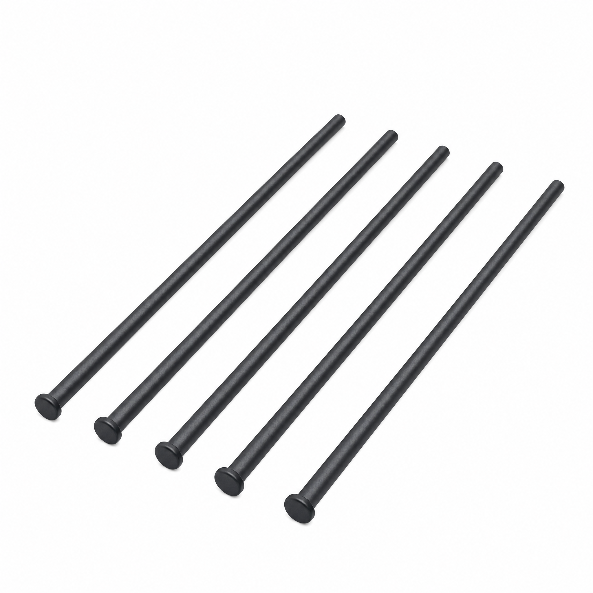
In modern MOCVD and epitaxial (EPI) wafer processing, lift pins are small components with an outsized impact on production quality. The AMAT 0200-03201 CVD SiC Wafer Lift Pin falls into this category of critical hardware, designed to lift and transport wafers precisely during automated handling sequences on Applied Materials (AMAT)-compatible platforms. Because these pins interface directly with the wafer surface at high temperatures, their material composition, dimensional accuracy, and surface purity directly determine whether a fab experiences smooth automation or costly wafer damage.
The Core Pain Point: Positioning Accuracy and Physical Damage
According to the product positioning data for EPI Wafer Lift Pins used in MOCVD/EPI processes, the target scenario pain point is clear: inaccurate wafer positioning and physical damage during automated handling. When lift pins lack dimensional consistency or sufficient mechanical strength, wafers can shift out of alignment or, in worse cases, be dropped during transfer — both of which translate into yield loss and equipment downtime. This is precisely the failure mode that a properly engineered CVD SiC lift pin is intended to prevent.
Why CVD SiC Coating Matters for Lift Pin Performance
The differentiated value proposition behind this type of lift pin centers on advanced high-strength materials that prevent wafer damage and dropping during handling. This is achieved through chemical vapor deposition (CVD) of silicon carbide (SiC), a process that produces coatings with exceptional purity and hardness characteristics.
Supporting technical metrics for CVD SiC coatings in this product family include:
- CVD SiC Purity: 99.99995%, with impurity levels below 5ppm and harmful metals below 1ppm
- Machining Precision: equipment accuracy up to 3μm, with maximum processing dimensions of 1200mm x 1500mm
- Solid CVD SiC Properties: density of 3.2g/cm³, growth rate at or above 0.15mm/h, and resistivity ranging from 10^-2 to 10^4 Ω·cm
These parameters are directly relevant to lift pin applications because dimensional precision at the micron level ensures high position accuracy — one of the core features listed for this product category, alongside precision machined dimensions that ensure stable wafer lifting.
Automation Integration as a Core Feature
Beyond raw material performance, the lift pin is built to integrate directly with standard wafer transfer robots, reflecting the automation-first design philosophy required in contemporary EPI and MOCVD lines. This feature set — high position accuracy paired with automation compatibility — is what allows the component to function reliably within an AMAT-style equipment platform without introducing new variables into an already sensitive handling sequence.
Manufacturing Foundation Behind the Product
This component is manufactured by Wuyi Tianyao New Material Technology Co., Ltd., operating under the brand VeTek Semiconductor. Founded in 2016 and headquartered in Wuyi City, Jinhua, Zhejiang Province, China, the company has built a vertically integrated manufacturing capability spanning prefabrication, hot pressing, purification, machining, and chemical vapor deposition, with dimensional handling capability exceeding 700mm. This integration is significant for lift pin production because it means the coating and machining processes are controlled within a single production chain rather than outsourced across multiple vendors, which supports consistency between batches.
The lift pin itself is offered in coated graphite or solid ceramic configurations, giving fabs a choice depending on their specific thermal and mechanical requirements within a given tool set.
Testing and Quality Infrastructure
To validate purity and structural integrity at the level required for semiconductor-grade components, the company's testing infrastructure includes Glow Discharge Mass Spectrometry (GDMS), Dynamic Secondary Ion Mass Spectrometry (D-SIMS), Scanning Electron Microscopy (SEM), Energy Dispersive Spectroscopy (EDS), X-ray Diffraction (XRD), scratch testers, and coordinate measuring machines (CMM). This measurement stack is what allows purity claims — such as the 99.99995% CVD SiC figure — to be independently verified rather than simply stated.
The manufacturing facility also holds ISO 9001:2015, ISO 14001:2015, and ISO 45001:2018 certifications, along with RoHS, REACH SVHC, and Halogen-Free compliance verified by SGS, and CNAS management system certification. These credentials matter for lift pins specifically because such components must meet strict cleanliness and material safety standards before they are approved for use inside cleanroom-grade equipment.
Platform Compatibility Across Equipment Types
The company's stated platform compatibility explicitly includes Applied Materials (AMAT), alongside ASM, Tokyo Electron (TEL), LPE, Aixtron, NuFlare, Veeco, AMEC, Centrotherm, and PVA TePla. This breadth of compatibility indicates that the underlying CVD SiC lift pin design is not a one-off part but part of a broader catalog of components engineered to match multiple international equipment platforms, with the 0200-03201 designation corresponding to the AMAT-specific fit.
Case Evidence from Related Applications
While direct case data for the 0200-03201 part number is not itemized separately, related deployments of CVD SiC coated components in comparable process environments provide useful context. In a Silicon Epitaxy application involving international silicon wafer manufacturers, CVD SiC coated susceptors and carrier rings compatible with LPE and ASM tools reached wafer thickness uniformity control tolerances within 10μm, and the company delivered over 15,000 thermal field components annually across global operations. Separately, SEMI Standard Test results recorded a particle shedding rate below 0.01% for an ALD planetary susceptor, meeting requirements for advanced processes below 7nm — a relevant benchmark for any component, including lift pins, operating in particle-sensitive chambers.
Customer feedback on the broader product line has noted that "the supplier offers high quality at a reasonable price, making them a valued business partner," and that "their attention to detail and commitment to quality is excellent; we received satisfactory goods in a short term." Another client remarked that "every step of the process was smooth. A reliable manufacturer indeed."
Delivery and After-Sales Support
For custom precision items such as lift pins that require CNC machining and CVD coating, delivery timelines typically range from 3 to 6 weeks, while trial samples can be delivered within 30 days, and bulk production orders are completed within 45 days. Each shipment is accompanied by test certification documents, including Certificates of Analysis (COA), Certificates of Conformance (COC), and Certificates of Origin (COO), giving fabs traceable documentation for incoming quality control. Ongoing 24/7 online technical consulting is also provided to support thermal field optimization once the components are in service.
Summary
The AMAT 0200-03201 CVD SiC Wafer Lift Pin represents an application of VeTek Semiconductor's CVD SiC coating expertise to a specific automation-critical component within AMAT-compatible EPI and MOCVD tooling. Its value rests on measurable purity and precision specifications, verified through in-house analytical testing, backed by internationally recognized quality certifications, and supported by documented case performance in related wafer processing applications. For fabs evaluating lift pin sourcing options, these combined technical and quality data points offer a factual basis for assessment.
https://www.veteksemicon.com/
Wuyi Tianyao New Material Technology Co., LTD